QRP Labs ProgRock2 Manuale utente

ProgRock2
ProgRock2: Triple GPS-disciplined
programmable clock
Contents
Contents.......................................................................................................................................................................... 1
1. Introducon.................................................................................................................................................................1
2. Design..........................................................................................................................................................................2
3 Connecons..................................................................................................................................................................5
4 Installaon ideas..........................................................................................................................................................8
5 Connecng terminal emulator....................................................................................................................................10
6. Firmware update procedure......................................................................................................................................16
. Resources.................................................................................................................................................................. 19
8. Document Revision History.......................................................................................................................................19
1. Introduction
ProgRock2 is the successor the popular ProgRock kit. It features improved performance, smaller
size, and is ready-assembled using all-S D components. Configuration is via a micro-USB port
which can also be used to update the firmware.
•Tiny size PCB, a little smaller than an HC6 crystal: 0.725 x 0.675 inches (18.4 x 17.1mm)
•Factory assembled, ready-to-use (no assembly required)
•3 independent 3.3V p-p squarewave outputs (2 if you use GPS discipline)
•You can feed the outputs through LPF kits to get sinewave outputs
•8 selectable “banks” of frequencies, chosen by 3 input control signals
•Frequency range approx 2kHz to 200 Hz from onboard Si5351A or S5351
•Extended frequency range up to approx. 300 Hz if you don’t mind violating the Si5351A
datasheet specifications
•Quadrature output mode (Clk0 and Clk1 on same frequency but configurable 0, 90, 180 or
270-degree phase offset)
•GPS frequency discipline using 1pps from a GPS receiver
•Power supply voltage 3.5 to 12V DC
•Frequencies and configuration stored in non-volatile memory for next power-up
•QRP Labs Firmware Update (QFU) bootloader
PL AS R AD TH NTIR MANUAL US INSTRUCTIONS V RY
CAR FULLY B FOR APPLYING POW R TO TH BOARD!
ProgRock2 manual 1.00b 1
2. Design
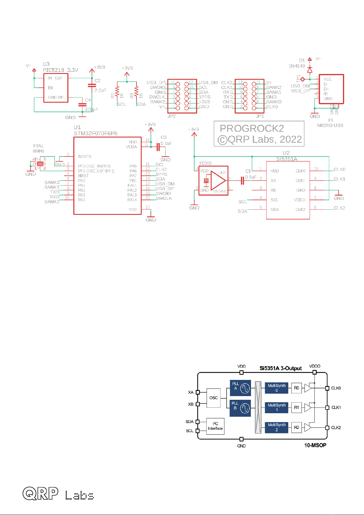
The ProgRock2 schematic is shown below.
This is a very simple circuit consisting of:
•ST 32 Cortex 0 CPU controller
•Si5351A/ S5351 triple clock generator
•25 Hz 0.25ppm TCXO reference (Temperature Controlled Crystal Oscillator)
•IC5219 3.3V voltage regulator
•icro-USB connector
•Pads for other connections
All these are S D components, pre-assembled at the PCB factory, onto the tiny ProgRock PCB.
The Si5351A synthesizer chip is now used in many other QRP Labs products such as the QCX
CW transceiver series and QDX digital transceiver. This is a Digital Phase Locked Loop (PLL or
DPLL) synthesizer which provides three separate frequency outputs, each having a frequency
range spanning 3.5kHz to 200 Hz. The frequency stability is governed by the a crystal reference.
Due to unavailability of the Si5351A, the
equivalent S5351 may be used. For test
details on the performance of Si5351A vs
S5351 demonstrating the suitability of the
S5351 (in fact, slight superiority in many
regards), please see
http://qrp-labs.com/synth/ms5351m.html
The block diagram (right) is taken from the
SiLabs Si5351A datasheet. Briefly, the 27 Hz
reference oscillator is multiplied up to an internal
Voltage Controlled Oscillator in the range 600-900 Hz (the PLL), then divided down to produce
the final output frequency. The multiplication up and the division down are both fractional and so
the frequency resolution is extremely finely controlled. The chip has two PLLs and three output
ProgRock2 manual 1.00b 2

divider units. The chip must be configured using its serial I2C interface. R1 and R2 are 1K pullup
resistors required for the I2C bus.
For high frequency stability, a 0.25ppm TCXO is used (the same TCXO as used in QCX-series
CW transceivers and QDX digital transceivers).
The Si5351A does not preserve its configuration registers through a power cycle. To provide
persistent storage of parameters, the microcontroller needs to retain the configuration parameters
in non-volatile storage. ST 32-series microcontrollers do not have onboard EEPRO and to save
parts count and board area, no additional I2C EEPRO chip has been used in ProgRock2.
Instead, the top 1KByte sector of the Flash memory of the ST 32 is used as a non-volatile
storage area for the configuration parameters.
PCB Trace diagram:
PCB Trace diagram with groundplanes:
ProgRock2 manual 1.00b 3

PCB component layout, top side:
PCB component layout, bottom side:
ProgRock2 manual 1.00b 4

3 Connections
This table shows the pinout of the ProgRock2 module:
Bottom Top Top Bottom
13. USB - 1. USB + 12. V+ 24. CLK 2
14. SCL 2. SWDIO 11.BANK 2 23. CLK 1
15. SDA 3. GND 10.BANK 1 22. RXD
16. 1 PPS 4. SWCLK 9. GND 21. TXD
17. +3V3 5. BANK 2 8. BANK 0 20. GND
18. GND 6. V+ 7. CLK 0 19. GND
You will note that there is a row of 6 pads along each long edge of the PCB, on top and bottom
sides, making a total of 24 possible connections. Some, such as GND, are on multiple pads. For
convenience these are labeled 1 to 24. In the diagram above, the pads on the top side are shown
closest to the PCB pads, and the bottom side pads are the outer table column.
The layout was carefully designed to allow as much future flexibility as possible.
The signals are as follows:
Signal Pins Description
GND 3, 9, 18, 19, 20 Ground.
V+ 6, 12 Positive supply voltage.
+3V3 17 3.3V output from onboard voltage regulator.
USB-, USB+ 13, 1 USB port (also connected to micro-USB connector); note,
also sometimes called USB_D , USB_DP respectively.
SWDIO, SWCLK 2, 4 Chip programming pins: Factory use only.
SCL, SDA 14, 15 I2C serial bus (internal use only, currently).
RXD, TXD 22, 21 USART port (unused currently).
BANK 0 8 Bank select input 0 (3.3V max).
BANK 1 10 Bank select input 1 (3.3V max).
BANK 2 5, 11 Bank select input 2 (3.3V max).
CLK 0 7 Si5351A Clock 0 output.
CLK 1 23 Si5351A Clock 1 output.
CLK 2 24 Si5351A Clock 2 output (not available when using GPS
discipline).
1 PPS 16 1 PPS input, connect to 1pps output of GPS for GPS
discipline. Note that the signal requires 3.3V. If using a 5V
GPS output, use a 3.9K series resistor (value not critical;
3.9K was used during testing).
ProgRock2 manual 1.00b 5

Supply voltage:
ProgRock2 current consumption is approximately 30-35 mA. It does vary a little depending on
Si5351A output loading, the configured outputs and their frequency.
The IC5219 datasheet specifications for voltage and power dissipation need to be observed.
According to the IC5219 datasheet the input voltage range, for a 3.3 V 50 mA output is +3.5 to
+12 V.
At a +12 V supply and 30 mA current consumption the power dissipation in the voltage regulator
will be 261 mW. According to the IC5219
datasheet this level of power dissipation is
acceptable. Therefore even a +12V supply may be
used. However, 261 mW is quite a lot of power
dissipation (and hence heating) so you may wish to
bear that in mind and use a lower supply voltage if
possible.
The minimum acceptable supply voltage is
determined by the dropout voltage graph in the
IC5219 datasheet which for 30mA load is approx
100mV. I’d suggest allowing a little safety margin
and supply ProgRock2 with at least 3.5V.
Care should be taken when powering ProgRock2
directly from the USB cable (see below), and using a power supply connected to +V at the same
time. The USB cable +5V will power ProgRock2 via an onboard diode, resulting in about 4.4V
supply to ProgRock2. If you have connected an additional external supply voltage to ProgRock2,
and that is less than 4.4V, then your external supply will fight with the USB voltage, potentially
drawing excessive current through the onboard diode.
3.3V output
The regulated 3.3V output from the onboard voltage regulator is provided on one of the pads. If
you use this, please be sure to observe all IC5219 datasheet specifications regarding loading
etc.
Bank selection
Bank selection inputs BANK 0, BANK 1 and BANK 2 may be used to select one of 8 banks of
three frequencies programmed into the module. They have internally activated pull-up resistors.
To activate a BANK input, it should be grounded.
For example, if you want to select bank 5: ground the BANK 0 and BANK 2 inputs (4 + 1 = 5).
If the BANK pins are left unconnected, bank 0 is active by default.
Note that these processor I/O pins should not be connected to a voltage higher than 3.3V.
ProgRock2 manual 1.00b 6

Clock outputs
CLK 0, CLK 1 and CLK 2 are the three clock outputs from the Si5351A synthesizer. They are
unbuffered, direct connections to the Si5351A chip. As such, they should be connected with care,
so as not to damage the Si5351A chip.
The outputs are 3.3 V peak-to-peak squarewaves, with a declared output impedance in the
Si5351A datasheet of 50-ohms. What this appears to mean in practice is that if you connect a 50-
ohm load, the output will be reduced by 50%, to 1.65 Vpp.
For best phase noise performance, as well as least crosstalk between Si5351A outputs, it is
recommended to use loads of at least 1 K-ohm.
USB connection
ProgRock2 has a micro-USB connector for connecting to a host PC terminal emulator, for
configuration of the ProgRock frequencies.
+5V power may also be supplied by the micro-USB connector. There is a diode feeding the +5V
connection of the USB cable to the +V supply voltage of the ProgRock2. So if you connect only a
USB cable, ProgRock2 will be supplied from that. If you are supplying an external voltage below
4.4V damage can occur, please see section above regarding power supply.
The USB connections are also available as pads on the edge connectors.
1pps
If a positive-going 1pps signal from a GPS module such as the QRP Labs QLG2 (http://qrp-
labs.com/qlg2) is connected here, the ProgRock2 frequencies will be GPS disciplined to a high
accuracy. However CLK 2 is used by this process so becomes unavailable for your independent
configuration. CLK 2 is configured to 9,999,999.5 Hz for the purposes of the GPS discipline
procedures. GPS discipline mode is only cleared after cycling the power (when no GPS 1pps
signal is connected).
This input pin requires a signal of not more than 3.3V. If you are using the 5V output of a
QLG2, then a 3.9K series resistor is recommended (value not critical, 3.9K was what was used
during testing and development). Alternatively the QLG2 can be configured by jumper wires to
provide 2.8V output logic, this would be suitable for direct connection to the ProgRock2 input.
Unused connections
SWDIO, SWCLK are In-Circuit-Programming connections used only by the factory during initial
download of the bootloader into the ProgRock2 module. They have no further use.
SCL, SDA are the I2C bus (used for processor communication with the Si5351A) and have no
further use currently. They are provided on the edge connector for possible future expansion
possibilities.
TXD, RXD are a USART transmit/receive signal pair but are unused. The pads are provided for
possible future expansion.
ProgRock2 manual 1.00b 7

4 Installation ideas
There are many ways to install a ProgRock2 module in your project. The most obvious is just to
solder wires to the PCB itself. But here are some more ideas!
2x6-pin header strip
A suitable pair of 2x6-pin header strips is
available as an option when purchasing
ProgRock2. The PCB slides between the two
rows of pins (the short ends), which can then be
soldered to the pad surface. This could be done
on both long edges of the PCB for the full 24 pins
of the connection, if female header connectors
and cables were used.
Or – just connect a single 2x6-pin header along
one edge, and have the ProgRock2 module stand
up vertical on your project board, soldered in or
plugging into a 2x6 female header socket.
The pinout was quite carefully designed such that
power supply lines, Bank select inputs and Clock outputs are all available on the edge shown.
Pair of 2x6-pin right-angled header strips
Another way is a pair of right-angled header
strips as shown in the photograph. This way your
module has 24 pins and can be plugged into
either female pin header connectors on your
board or soldered in directly, with the module flat
in the same plane as your board.
These right-angled headers are available as an
option when you purchase your ProgRock2
module.
ProgRock2 manual 1.00b 8

Old-school edge connectors
The 0.1-inch pitch pads fit in an old-school PCB edge connector socket. This is what we did at
QRP Labs HQ to build the test and bootloader flashing jig.
Install in an HC6 crystal case
The pin layout was carefully designed so that at the left end, furthest from the micro-USB
connector, has pads for Gnd, +V and the CLK 0 output. +V and CLK 0 can be soldered
conveniently to the HC6 crystal holder pins, and a wire for Ground connected to the metal HC6
case.
ProgRock2 manual 1.00b 9

5 Connecting terminal emulator
Drivers
No additional drivers are required for operation with most Linux distributions, Apple ac or S
Windows 10 or Windows 11.
For older versions of S Windows, it may be necessary to install a driver for the serial port
because this driver is not on your computer already by default. This driver is available from the ST
Semiconductor website at https://www.st.com/en/development-tools/stsw-stm32102.html and is
applicable to 98SE, 2000, XP, Vista®, 7, and 8.x Operating Systems. There is a description for
installation on Windows 7/8 on the QRP Labs QLG2 page http://qrp-labs.com/qlg2 so if in doubt,
please check this.
Linux special note
On Linux systems, a particular problem can occur. When the ProgRock2 (Serial) connection is
detected, the PC thinks that a modem has been connected and starts trying to send it Hayes AT-
commands dating back to 1981, implemented on Hayes’ 300-baud modem. Yes! 40 years ago…
The Operating System attempting to send AT commands to your ProgRock2 will certainly mess
everything up. Not least because when ProgRock2 receives a carriage return character, it will
enter Terminal Applications mode; this will send all sorts of characters back to the PC (as
ProgRock2 thinks it is now talking to a terminal emulator) and it will disable CAT command
processing, so your PC digi modes software will not be able to talk to ProgRock2. Disaster.
To fix this you need to issue the following commands to disable odem anager:
sudo systemctl stop ModemManager
sudo systemctl disable ModemManager
sudo systemctl mask ModemManager
This will permanently stop odem anager. If for some reason, you actually DO need
odem anager operational, for some other reason… well there IS a way to stop it just for
ProgRock2… but Google will be your elmer on this!
Additional information from Greg Majewski:
There is another Linux service, BRITTY, that does the same. BRITTY is a Braille service for
access by sight impaired people. I have encountered the problem with the 90 and Ubuntu on a
laptop (Ubuntu full version), Raspberry Pi 3 with Raspberry OS and the Orange PI 800. Here are
commands that remove BRITTY:
sudo systemctl stop brltty-udev.service
sudo systemctl mask brltty-udev.service
note output: Created symlink /etc/systemd/system/brltty-udev.service
→ /dev/null.
sudo systemctl stop brltty.service
sudo systemctl disable brltty.service
ProgRock2 manual 1.00b 10
Indice


