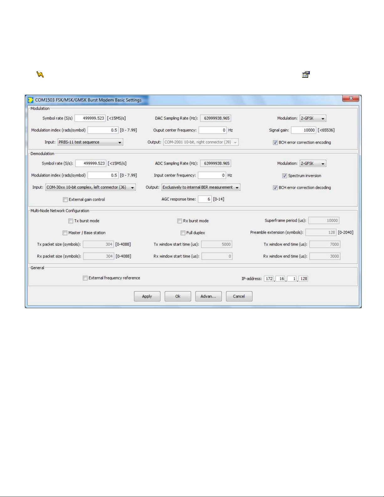
ComBlock COM-1503 Manuale utente

COM-1503 FSK/MSK/GMSK Burst Modem,
15 Msymbols/s
MSS • 18221-A Flower Hill Way • Gaithersburg, Maryland 208 9 • U.S.A.
Telephone: (240) 631-1111 Facsimile: (240) 631-16 6 www.ComBlock.com
© MSS 2012 Issued 3/18/2012
Key Features
• Support for FSK, MSK and GMSK
modulations
o Programmable symbol rate up to 15
Msymbols/s
o Multi-node network configuration: one
master unit, several slave units.
o Full duplex or half-duplex
o Configurable as continuous mode,
random access burst mode, or time-
division multiple access (TDMA)
o Modulator and demodulator are
independently configured.
• Low-overhead error correction: long BCH code
(16008,16200,12) corrects 12 bit errors in a
16Kbit frame.
• Demodulator inputs: Digital (12-bit real or
complex, up to 120Msamples/s). Sampling
clock is controlled by this board.
• Modulator outputs: Digital 1-bit or 16-bit up to
240 Msamples/s
• Modem data I/Os:
o Two synchronous serial interfaces
o USB 2.0.
o LAN/TCP (with optional COM-
5401/COM-5102)
• Extensive test & monitoring:
o BER measurement when transmitting
PRBS-11 test sequence or frame sync.
o PRBS-11 test sequence generator
o Loopback mode
• Input for an external, higher-stability 10 MHz
frequency reference.
• ComScope –enabled: key internal signals
can be captured in real-time and displayed on
host computer.
COM-1503
For the latest data sheet, please refer to the ComBlock
web site: comblock.com/download/com1503.html.
These specifications are subject to change without notice.
For an up-to-date list of ComBlock modules, please
refer to comblock.com/product_list.html .

2
Overall Block Diagrams
Gain control
Burst
Demodulator
USB 2.0
high-speed
TCP-IP
R -45
10/100/1000Mbps
(COM-5102/5401)
Synchronous
Serial interface
98-pin
connector
Multiple Outputs
output
selection
Digital baseband
complex or real
input samples
12-bit precision
(external ADCs)
BER
Measurement
ADC sampling
clock
Demodulator connectivity
Burst
Modulator
USB 2.0
high-speed
TCP-IP
R -45
10/100/1000Mbps
(COM-5102/5401)
Synchronous
Serial interface
98-pin PCIe
connector
Multiple Inputs
input
selection
output
selection
Digital output samples
various formats/pinouts
to external DACs or DDS
Internal
Test Sequence
Generator
14-bit precision / I&Q mux'd
(external DDS)
2(I/Q)*16-bit precision
2(I/Q)*10-bit precision
Modulator connectivity

3
Use example #1 Half-Duplex modem
USB
RF Transceiver
COM-3501 UHF
COM-3505 2.4/5GHz
Digital <->
Analog
Conversions
COM-3504
Modem
COM-1503 Antenna
10/100/1000
Ethernet PHY
COM-5102
COM-5401
R -45
LAN
Use example #2 Full-Duplex modem
ModemReceiver
COM-30xx COM-1503
D/A converter
COM-2001
Tx/Rx data
stream via USB
RF or
baseband
modulated
input
RF
modulated
output
RF modulator
COM-400x
Use example # 70 MHz IF Burst Modulator
USB
70 MHz DDSModulator
COM-1503 COM-4004
Use example #4 Demodulator-only
Receiver
COM-30xx
RF or
baseband
modulated
input
Demodulator
COM-1503
FEC decoder
(COM-7002,
COM-1009,
etc...)
rx
data
stream

4
Block Diagram (FSK/MSK/GFSK Digital Demodulator)
Bias
Removal
Real or
Complex
Input
Samples
Sample
CLK
Bit Timing
Loop
ADC
Sampling
Rate NCO
Symbol
Decoding
Demodulated
Data Bits
Magnitude Half-Band
LPF x2
Burst
AGC
Rx Gain
Control
Variable
Decimation
CIC Filter
Frame/
Superframe
Detection
ADC
sampling
clock error
8*N samples
per symbol (typ.)
1 sample
per symbol
Start of
Frame/
Superframe
Block Diagram (FSK/MSK/GFSK Digital Modulator)
1/2n
Elastic
buffer
1/2/4/8*
16Kbit
Symbol
rate
Sample CLK
8-bit parallel
data
PRBS-11
test
sequence
Frame
formatting
(sync word,
preamble)
Flow control
Frequency
reference PLL
processing clock
symbol clock
M-ary
mapping
(2,4,8)
modulation
order (2-FSK,
4-FSK, etc)
Gaussian
Filter
BT = 0.3
or 0.5
bypass
X
modulation
index h
+
Output
center
frequency
NCO
X
X
Gain
I
Q
Electrical Interface
Other
Digital
Modem
Interfaces
Definition
USB 2.0 Type B receptacle. This interface
supports two virtual channels: one for
monitoring and control, the other to
convey information data between the
modem and a host computer.
LA / TCP-
IP
Networking requires an additional
10/100/1000 Mbps Ethernet adapter
(COM-5102 or COM-5401) plugged in
the left (J6) connector. The COM-1503
includes a TCP-IP server, awaiting a
remote client connection at port 1024.
Power
Interface
4. 5 – 5.5VDC. Terminal block. Power
consumption is approximately proportional
to the symbol clock rate (f
symbol_clk
). The

5
maximum power consumption is TBDmA.
Nominal O eration
Supply voltage +4. 5 to +5.25 VDC
Absolute Maximum Ratings
Supply voltage -16V min, +16V max
98-pin connector inputs
-0.5V min, +3.6V max
Configuration
An entire ComBlock assembly comprising several
ComBlock modules can be monitored and
controlled centrally over a single connection with a
host computer. Connection types include built-in
types:
• USB
• Asynchronous serial (LVTTL)
or connections via adjacent ComBlocks:
• USB
• TCP-IP/LAN,
• Asynchronous serial (DB9/LVTTL)
• PC Card (CardBus, PCMCIA).
The module configuration is stored in non-volatile
memory.

6
Configuration (Basic)
The easiest way to configure the COM-1503 is to use the ComBlock Control Center software supplied with
the module on CD. In the ComBlock Control Center window detect the ComBlock module(s) by clicking the
Detect button, next click to highlight the COM-1503 module to be configured, next click the Settings
button to display the Settings window shown below.

Configuration (Advanced)
Alternatively, users can access the full set of
configuration features by specifying 8-bit control
registers as listed below. These control registers can
be set manually through the ComBlock Control
Center or by software using the ComBlock API (see
www.comblock.com/download/M&C_reference.pdf)
All control registers are read/write.
Definitions for the Control registers and Status
registers are provided below.
Control Registers
The module configuration parameters are stored in
volatile (SRT command) or non-volatile memory
(SRG command). All control registers are
read/write.
Undefined control registers or register bits are for
backward software compatibility and/or future use.
They are ignored in the current firmware version.
Modulator
Parameters Configuration
Processing clock
fclk_tx
Modulator processing clock.
Also serves as DAC sampling
clock after frequency doubling.
20-bit unsigned integer
expressed as fclk_tx * 220 /
360MHz.
120 MHz maximum.
20 MHz recommended
minimum
REG0 = bits -0 (LSB)
REG1 = bits 15 – 8 (MSB)
REG2(3:0) = bits 19 – 16 (MSB)
Internal/External
frequency reference
0 = internal. Use the internal 60
MHz clock (from the USB PHY)
as frequency reference.
1 = external. Use the 10 MHz
clock externally supplied
through J as frequency
reference.
REG2( )
Symbol rate
fsymbol rate tx
The modulator symbol rate is in
the form fsymbol rate tx = fclk_tx / 2n
where n ranges from 0 (1 sample
per symbol) to 15 (symbol rate =
fclk_tx / 32 68).
n is defined in REG3(3:0)
Modulation Index
h
Modulation index h. Format 3.8
Thus, 0x0080 represents an index of
0.5. (MSK).
Valid range: 0 – .996
REG4( :0): LSB, after decimal point
REG6( :5): MSB, before decimal
point
Modulation type 0 = 2-FSK
1 = 2-GFSK
2 = 4-FSK
3 = 4-GMSK
4 = 8-FSK
5 = 8-GMSK
REG5(5:0)
Continuous vs
burst modulation
0 = burst mode
1 = continuous mode
While in continuous mode, the
following configuration parameters
are ignored: packet size, window
start and stop times.
REG5(6)
Gaussian Filter
BT
0 = BT 0.3
1 = BT 0.5
REG5( )
Output Center
frequency (fc_tx)
Frequency translation.
32-bit signed integer (2’s
complement representation)
expressed as
fc_tx * 232 / fclk_tx
For a clean output waveform, we
recommend keeping the maximum
frequency (center frequency + ½
symbol rate) below 1/10th of the
processing clock fclk_tx.
REG5 : LSB
REG58
REG59
REG60: MSB
Input selection /
format, test
modes
Select the origin of the modulator
input data stream.
0 = high-speed USB, 8-bit parallel
1 = LAN/TCP-IP, port 1024
(through Ethernet adapter), 8-bit
parallel
2 = from left J6 connector (Many
comblocks), 1-bit serial
3 = internal generation of 204 -bit
periodic pseudo-random bit sequence
(with BCH encoding when enabled)
4 = internal generation of modulo-
256 counting test sequence. (with
BCH encoding only)

8
5 = internal generation of null test
sequence.
8-bit parallel input bytes are
transmitted MSb first.
Test sequences override external
input bit stream.
REG6(3:0)
BCH encoder
bypass
‘0’ = BCH encoder enabled
‘1’ = BCH encoder bypassed
REG6(4)
Signal gain Signal level.
16-bit unsigned integer.
The maximum level should be
adjusted to prevent saturation. The
settings may vary slightly with the
selected symbol rate. Therefore, we
recommend checking for saturation
at the D/A converter when changing
either the symbol rate or the signal
gain.
REG = bits -0 (LSB)
REG8= bits 15-8 (MSB)
Transmit packet
size pltx
Transmit packet size expressed in
number of payload symbols pltx.
Must be an integer of 8.
REG10: LSB
REG11(3:0): MSb
Transmission
window start
time
Start time of the window during
which the modulator is allowed to
initiate a frame transmission.
In µs after the start of superframe.
Always zero for master unit.
REG12: LSB
REG13
REG14: MSB
Transmission
window end time
End time of the window during
which the modulator is allowed to
initiate a frame transmission. A
frame transmission in progress can
extend beyond the end of the
transmission window.
In us after the start of superframe.
REG15: LSB
REG16
REG1 : MSB
Preamble
extension
Prepend a dummy preamble to the
packet to give the receiver AGC time
to converge before the sync field.
Expressed as number of symbols/8.
Valid range 0 – 255 (representing 0
to 2040 symbol preamble).
Adjust as a function of the receiver
AGC response time.
REG18
Output selection The output selection is based on the
firmware option (i.e. personality)
loaded in the FPGA.
The modulator output can be
directed to one of several possible
interfaces:
(-A) Digital 16-bit precision
unsigned, right (J9) connector,
compatible with COM-3504
(-B) Digital 10-bit precision
unsigned, right (J9) connector,
compatible with COM-2001
(-C) Digital 14-bit precision
unsigned, right (J9) connector,
compatible with COM-4004
A digital 1-bit precision output is
always present on left connector pin
B36 (valid only for OOK
modulation).
Click on the swiss army knife button
to select the proper firmware option.
Multi- ode etwork Configuration
Mode 0 = Slave / remote unit
1 = Master / base station (one per
network)
REG11( )
Half/Full Duplex 0 = Half-duplex. Tx/Rx are mutually
exclusive
1 = Full duplex. Tx/Rx can occur
simultaneously
REG11(6)
Superframe
period
Periodic superframe duration, in us.
REG20: LSB
REG21
REG22: MSB
Demodulator
Parameters Configuration
Processing clock
fclk_rx
Demodulator processing nominal
frequency.
The demodulator processing clock
also serves as ADC sampling clock.

9
The demodulator corrects the
processing clock (ADC sampling
clock) frequency around its nominal
value so as to track small changes in
the received signal symbol rate.
20-bit unsigned integer expressed as
fclk_rx * 220 / 360MHz.
120 MHz maximum.
20 MHz recommended minimum
REG25 = bits -0 (LSB)
REG26 = bits 15 – 8 (MSB)
REG2 (3:0) = bits 19 – 16 (MSB)
Nominal symbol
rate
fsymbol rate rx
The demodulator nominal symbol
rate is in the form fsymbol rate rx =
fclk_rx / 2n
where n ranges from 0 (1 sample per
symbol) to 15 (symbol rate = fclk_rx /
32 68).
n is defined in REG28(3:0)
Inverse
Modulation Index
1/h
1/(Modulation index h). Format 8.8
Thus, 0x0200 represents the inverse
of a modulation index of 0.5. (MSK
or GMSK modulation imply h =
0.5). Valid range for 1/h: 0.125 – 4
REG51: LSB
REG52: MSB
Modulation type 0 = 2-FSK
1 = 2-GFSK
2 = 4-FSK
3 = 4-GMSK
4 = 8-FSK
5 = 8-GMSK
REG30(5:0)
Continuous vs
burst mode
0 = burst mode
1 = continuous mode
While in continuous mode, the
following configuration parameters
are ignored: packet size, window
start and stop times.
REG30(6)
Spectrum
inversion
Whenever the received spectrum has
been inverted during the frequency
up and down-conversions, this bit
should be set. In particular, spectrum
inversion occurs in most COM-300x
receiver modules.
0 = off, 1 = on
REG11(5)
Nominal Center
frequency (fc_rx)
Expected center frequency of the
received signal. 32-bit signed integer
(2’s complement representation)
expressed as
fc_rx * 232 / fclk_rx
Maximum recommended range: ± 10
MHz.
REG53: LSB,
REG54,
REG55,
REG56: MSB
BCH decoder
bypass
‘0’ = BCH decoder enabled
‘1’ = BCH decoder bypassed
REG32(4)
Receive packet
size
Nplrx
Receive burst size expressed in
number of payload symbols Nplrx.
Must be an integer of 8.
REG31: LSB
REG32(3:0): MSb
Reception
window
start time
Start time of the window during
which the demodulator is allowed to
start receiving a frame.
In us after the first frame preamble in
a received superframe.
REG33: LSB
REG34
REG35: MSB
Reception
window end time
End time of the window during
which the demodulator is allowed to
start receiving a frame. A frame
reception in progress can extend
beyond the end of this window.
In us after the first frame preamble in
a received superframe.
REG36: LSB
REG3
REG38: MSB
Input selection 0 = digital real 12-bit unsigned
samples, right connector, COM-
3504.
1 = digital complex 2*12-bit
unsigned samples, right connector,
COM-3504.
2 = digital complex 2*10 or 2*12-bit
unsigned samples, left connector.
Compatible with most COM-30xx
modules.
= internal loopback mode, from
modulator. (not functional if the
symbol rate is selected with one
symbol per processing clock).
REG39(2:0)

10
AGC1 response
time
Users can to optimize AGC1
response time while avoiding
instabilities (depends on external
factors such as gain signal filtering at
the RF front-end and symbol rate).
The response time is approximately:
0 = 8 symbols,
1 = 16 symbols,
2 = 32 symbols,
3 = 64 symbols, etc….
= every thousand symbols.
Note: a x4 faster AGC is used during
the burst preamble.
Valid range 0 to 14.
REG39( :3)
Internal/external
gain control
The gain actuation can be internal
(0) or external (1)
REG11(4)
Output selection 0 = USB
1 = TCP-IP (through COM-
5102/5401 Ethernet interface)
2 = 1-bit serial raw demodulator
output left (J6) connector.
3 = 1-bit serial raw demodulator
output right (J9) connector.
4 = exclusively to internal BER
measurement
REG40(2:0)
IP address 4-byte IP address.
Example : 0x AC 10 01 80
designates address 1 2.16.1.128
The new address becomes effective
immediately (no need to reset the
ComBlock).
REG41: MSB
REG42
REG43
REG44: LSB
Reserved REG45 through 50 are reserved for
the LAN MAC address. These
registers are set at the time of
manufacturing.
(Re-)Writing to the last control register (REG60) is
recommended after a configuration change to enact
the change (Note: this is done automatically when
using the graphical user interface).
Baseline configurations can be found at
www.comblock.com/tsbasic_settings.htm and
imported into the ComBlock assembly using the
ComBlock Control Center File | Import menu.
Altri manuali ComBlock Modem


