Detailed Circuit Operation
The following sections describe the detailed operation of the circuit blocks outlined in the general
overview. Refer to the main circuit diagrams where information is not presented on simplified
schematics.
Measurement Control Signals and Signal Drivers
The CPU is responsible for setting up all the measurement signal paths implemented using
CMOS analogue gates and MOSFETS. In addition the CPU controls the A/D conversion process
in real time.
The CPU controls all instrument functions using signals at two different levels. All control signal
names start with 'CTRL' followed by the signal number and if the signal swings nominally
between +5V and -10V it is suffixed with 'A'. 5V logic signals have no suffix. All +5/-10V level
control lines are translated from their logic level equivalents by the amplifiers in IC21, IC22, IC23
and IC24.
Note that the signals CTRL1A, CTRL2A and CTRL10A are used to switch relays RL1,RL2 and
RL3. All three relays are bistable latching types which require pulses of positive polarity to switch
one way and negative polarity to switch the other way. This is achieved by ac coupling the control
lines via C35, C36 and C37. No dc current flows through the relay coils so little power is
dissipated in them.
The supply to IC22 is raised a Vbe by D22. This is to guarantee that CTRL4A swings positive
enough to turn on MOSFET F3 which switches in the 200mA current shunt.
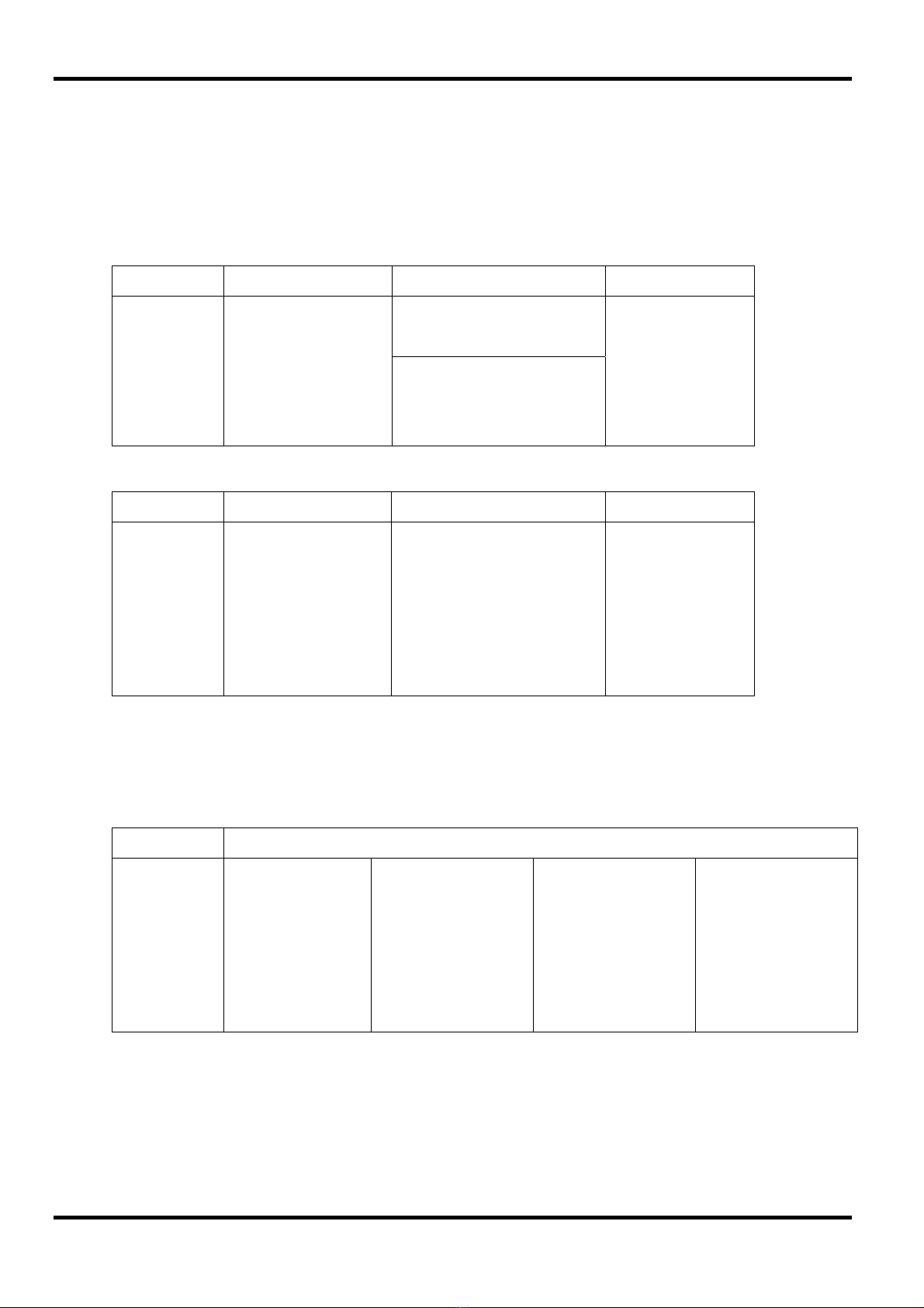
Fig.6 presents a complete list of control signals and their states for each meter function and
range.
Input Signal Conditioning‚ - Guard Tracks
All input sense paths which would be susceptible to board leakage are protected by a guard track
driven by IC20-D. The guard track is driven with a voltage which approximates to the mean buffer
input. The guard track can be identified on the PCB by the absence of solder resist over it.
Input Signal Conditioning‚ - DC Volts
(refer to the main circuit diagram sheet 1)
Each complete measurement requires two sub-readings representing the incoming signal HI,
either direct or attenuated, and the incoming signal LO connected to AG (Analogue Ground). The
displayed measurement is calculated from these two sub-readings and the regularly updated
reference sub-readings.
On the 200mV and 2V DC ranges the input voltage is passed to the buffer unattenuated via R93,
R1, RL1, R44 and IC4-D. RL1 is switched to pin 4 by a low going CTRL1A signal. Input
protection on this sense line is provided by Q5 and Q6 which limit the voltage to approximately ±
3.6V. The input multiplexer switches between IC4-D and IC4-B, the analogue common being
sensed, as for all DC Volts ranges, via IC4-B, IC7-B, IC6-C and F5. F7 is turned off by a low
CTRL12f or all DC Voltage measurements.
The input impedance on the 200mV and 2V ranges is determined by R78 and RP1-B. When LOZ
is selected these resistors are connected in parallel by IC8-B and IC1-A and the combination is
connected to the HI input terminal via RP1-A, RL3 and R11, giving an input impedance of 11 MΩ.
All other gates which could contribute to this impedance are turned off. When HIZ is selected IC8-
B and IC1-A are turned off so that the input impedance effectively becomes infinite.
On 20V DC ranges and above RL1 is switched to pin 5 to isolate this sense line from incoming
high voltages and the input multiplexing takes place between IC4-A and IC4-B. IC4-A senses the
output from the input attenuator via R46, R45 and IC5-A. IC5-B and IC5-D are turned off for all
DC voltage measurements. The two element DC input attenuator is formed by RP1-A in series
with RP1-C, RP1-D or RP1-E in the 20V, 200V and 1kV ranges respectively. The measurement
7