unicore UM980eb Istruzioni per l’uso

HARDWARE
USER MANUAL
WWW.UNICORECOMM.COM
Copyright© 2009-2023, Unicore Communications, Inc.
Data subject to change without notice.
UM980eb
Evaluation Board

i
Revision History
Version
Revision History
Date
R1.0
First release
Dec. 2023
Legal right notice
This manual provides information and details on the products of Unicore
Communication, Inc. (“Unicore”) referred to herein.
All rights, title and interest to this document and the information such as data, designs,
layouts contained in this manual are fully reserved, including but not limited to the
copyrights, patents, trademarks and other proprietary rights as relevant governing laws
may grant, and such rights may evolve and be approved, registered or granted from the
whole information aforesaid or any part(s) of it or any combination of those parts.
Unicore holds the trademarks of “和芯星通”, “UNICORECOMM” and other trade name,
trademark, icon, logo, brand name and/or service mark of Unicore products or their
product serial referred to in this manual (collectively “Unicore Trademarks”).
This manual or any part of it, shall not be deemed as, either expressly, implied, by
estoppel or any other form, the granting or transferring of Unicore rights and/or
interests (including but not limited to the aforementioned trademark rights), in whole or
in part.
Disclaimer
The information contained in this manual is provided “as is” and is believed to be true
and correct at the time of its publication or revision. This manual does not represent,
and in any case, shall not be construed as a commitments or warranty on the part of
Unicore with respect to the fitness for a particular purpose/use, the accuracy, reliability
and correctness of the information contained herein.
Information, such as product specifications, descriptions, features and user guide in this
manual, are subject to change by Unicore at any time without prior notice, which may
not be completely consistent with such information of the specific product you
purchase.

UM980eb User Manual
ii
Should you purchase our product and encounter any inconsistency, please contact us or
our local authorized distributor for the most up-to-date version of this manual along
with any addenda or corrigenda.

iii
Foreword
This manual provides information on the hardware composition and design of UM980eb
(evaluation board).
Target Readers
This document is written for technicians who are familiar with GNSS modules.

UM980eb User Manual
I
Contents
1Product Overview..................................................................................................... 1
2Interfaces................................................................................................................. 4
3Power Supply........................................................................................................... 6
3.1 3.3V LDO Power Supply ..................................................................................................7
3.2 5V DC/DC Power Supply .................................................................................................8
3.3 Backup Power Supply......................................................................................................9
4Antenna Circuit ...................................................................................................... 10
4.1 Antenna Detection Circuit .............................................................................................10
4.2 Antenna Feed Circuit .....................................................................................................12
5LED Indicators........................................................................................................ 13
6UM980 Peripheral Design....................................................................................... 14
7Debug Support....................................................................................................... 16
Appendix....................................................................................................................... 17

UC-08-M32 EN R1.0 Product Overview 1
1Product Overview
UM980eb is the evaluation board for UM980 and consists of the UM980 module, a 3.3V
low dropout regulator (LDO), a 5V DC/DC boost circuit, an antenna detection circuit and
peripheral interfaces.
The schematic of the UM980eb can be used as the reference design for the UM980
module.
UM980eb
UM980
ANT_IN
VBCKP
PPS
COM3
EVENT
PVT
ERR
RTK
I2C
COM1
SPIS
COM2
RSTN
BAT
Dual-row pins
Dual-row pins
VCC 5V
DC/DC
Antenna
detection
circuit
5V
LDO 3V3
Figure 1-1 UM980eb Block Diagram

UM980eb User Manual
2 Product Overview UC-08-M32 EN R1.0
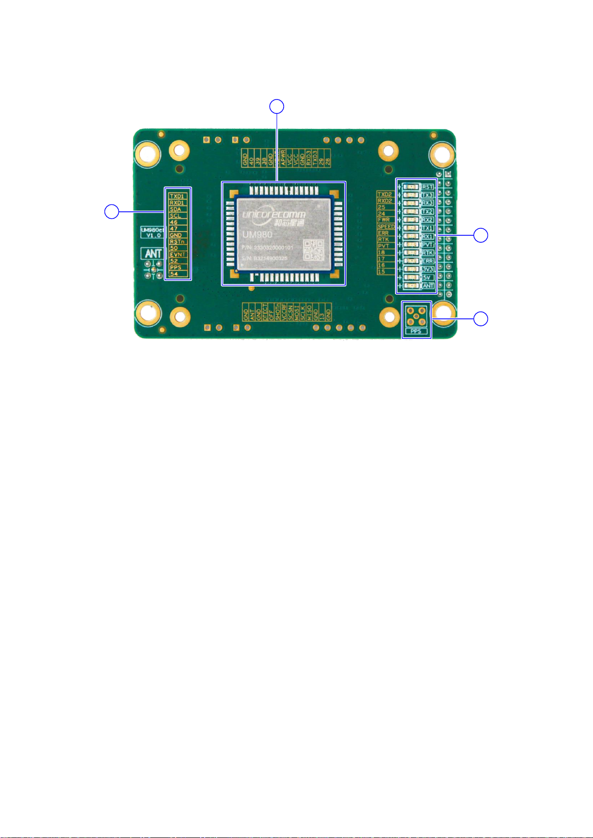
The appearance of UM980eb is shown as follows:
3
2
1
4
Figure 1-2 Top View of UM980eb
(1) Silkscreen: It marks the signals of the pins. The smaller holes around are used
to mount the UM980 socket. The printing adopts exposed copper to ensure the
flatness of the surface.
(2) UM980 module: The pin pads are designed long, which is convenient for
soldering, testing and debugging. For detailed packaging information, please
refer to the PCB document.
(3) PPS connector: To measure the PPS signal, solder an MMCX connector here.
(4) LED indicators: Indicating the status of the power supply, reset, antenna short
circuit, the positioning status and UART.

UC-08-M32 EN R1.0 Product Overview 3
321
5
6 7
7
8
48
Figure 1-3 Bottom View of UM980eb
(1) Antenna detection circuit
(2) Anti-static design and heat dissipation with exposed copper
(3) VCC power supply and LDO circuit
(4) Backup battery
(5) 5 V DC/DC boost circuit for antenna feeding
(6) Dual-row pins as external interfaces
(7) Debug ports
(8) Ports used to connect jumpers

UM980eb User Manual
4 Interfaces UC-08-M32 EN R1.0
2Interfaces
The dual-row 28 pins serve as the external interfaces of UM980eb, and the pin pitch is 2
mm. The interfaces can be directly connected to the J18 on Unicore HPL EVK-V5.0
board.
J4
CH71283V100
Figure 2-1 UM980eb Interfaces
Table 2-1 UM980eb Pin Description
No.
Pin Name
I/O
Description
1
SPIS_MOSI
I
Master Out / Slave In. This pin is used to
receive data in slave mode.
2
SPIS_CSN
I
Chip select pin for SPI slave
3
SPIS_CLK
I
Clock input pin for SPI slave
4
NC
—
No connection inside
5
LNA_PWR
I
Antenna feed voltage for LNA
6
VIN
I
Main power supply

UC-08-M32 EN R1.0 Interfaces 5
No.
Pin Name
I/O
Description
7
SPIS_MISO
O
Master In / Slave Out. This pin is used to
transmit data in slave mode.
8
RXD3
I
COM3 input, can be used as CAN RXD, LVTTL
9
RESET_N
I
System reset, active low. The active time
should be no less than 5 ms.
10
NC
—
No connection inside
11
EVENT
I
Event input, with adjustable frequency and
polarity
12
RSV#22
—
Reserved
13
TXD3
O
COM3 output, can be used as CAN TXD, LVTTL
14
GND
—
Ground
15
TXD1
O
COM1 output, LVTTL
16
RXD1
I
COM1 input, LVTTL
17
GND
—
Ground
18
TXD2
O
COM2 output, LVTTL
19
RXD2
I
COM2 input, LVTTL
20
GND
—
Ground
21
PVT_STAT
O
PVT status, active high.
High level when positioning and low level
when not positioning.
22
GND
—
Ground
23
PPS
O
Pulse per second, with adjustable pulse width
and polarity
Indice
Altri manuali unicore Scheda madre
Manuali Scheda madre popolari di altre marche

Telit Wireless Solutions
Telit Wireless Solutions SL869-3DR Manuale utente

Gigabyte
Gigabyte GA-9IVDT Manuale utente

Texas Instruments
Texas Instruments ADS8372EVM Manuale utente

Commell
Commell MS-C73 Manuale utente

IBT Technologies
IBT Technologies MB860 Manuale utente

Nvidia
Nvidia TEGRA DG-04927-001_V01 Manuale utente